CH7521A
- If you have questions about the product, or encounter any, you can register the site account,
- Then go to the technical support forum to ask for help.

|
|
||||
|
|
|||||
|
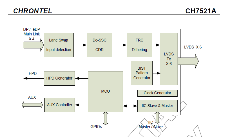
Chrontel’s CH7521A is a low-cost,
low-power semiconductor device that translates the DisplayPort signal to the
LVDS in form of RGB. This innovative DisplayPort receiver with integrated 6
channel LVDS transmitters is specially designed to target the Pro-AV and
Automotive market segments. Leveraging the DisplayPort’s unique source/sink
“Link Training” routine, the CH7521A is capable of instantly bring up the
video display to the LCD when the initialization process is completed between
CH7521A and the graphic chip.
The CH7521A is designed to meet the
DisplayPort specification version 1.2 and the Embedded DisplayPort
Specification version 1.2. The 4 Main Link Lanes receiver supports input with
data rate running at 1.62Gb/s, 2.7Gb/s or 5.4Gb/s, and can accept digital RGB
signal for LVDS output up to 7680x1080@60Hz or 4800x2160@60Hz.
The CH7521A will convert the DisplayPort
signal to LVDS output after DisplayPort Link Training is completed. This
feature can be achieved by loading the panel’s EDID and the CH7521A’s
configuration settings in the serial external BOOT ROM connected to the
CH7521A. During system power-up and upon completion of the DisplayPort Link
Training through AUX Channel, CH7521A will generate LVDS signal according to
the panel power-up timing sequencing stored in the external BOOT ROM.
Advanced Region CRC checking and signal
failure detection module and the related interrupt mechanism is incorporated
in CH7521A, which is specially designed to reduce the risk of signal
transmission error in normal consumer or industrial operation.
|
PCB Layout and Design Guide for CH7521A, AN-B059 rev0.1
Copyright © 1998-2017 Chrontel, Inc. All Rights Reserved. Privacy protection Legal statement