CH7516
- If you have questions about the product, or encounter any, you can register the site account,
- Then go to the technical support forum to ask for help.

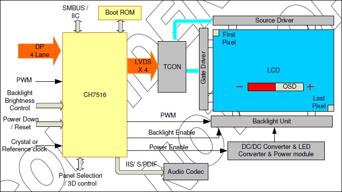
Chrontel’s CH7516 is a low-cost, low-power semiconductor device that translates the DisplayPort signal to the LVDS in form of RGB/YCbCr 4:4:4/YCbCr 4:2:2. This innovative DisplayPort receiver with integrated 4 channel LVDS transmitters is specially designed to target the All-In-One PC and the notebook market segments. Leveraging the DisplayPort’s unique source/sink “Link Training” routine, the CH7516 is capable of instantly bring up the video display to the LCD when the initialization process is completed between CH7516 and the graphic chip.
The CH7516 is designed to meet the DisplayPort Specification version 1.1a. The 4 DisplayPort Main Link Lanes receiver supports input with data rate running at either 1.62Gb/s or 2.7Gb/s, and can accept digital RGB signal for LVDS output up to QSXGA 2560x2048@60Hz. With advanced 3D processingmodule integrated, The CH7516 can support up to 1920x1080@120Hz 3D display mode, with programmable emitter control signal and 3D LCD panel’s backlight control signal output.
The Backlight Enable control and the PWM are the two kinds of backlight control functions designed in the CH7516 Panel power control module. The brightness control commands sent through AUX Channel can be dynamically translated by CH7516 and converted into LCD backlight control signal. Alternatively, the brightness control commands can be input from the PWM in and GOIO pin of Backlight Brightness Control. The CH7516 will save the last setting of brightness level into the external BOOT ROM and restore it upon power up. The CH7516 can dynamically adjust backlight brightness according to video stream to save power consumption and it supports OSD display in this way.
The CH7516 will immediately convert the DisplayPort signal to LVDS output after DisplayPort Link Training is completed. This feature can be achieved by loading the panel’s EDID and the CH7516’s configuration settings in the serial external BOOT ROM connected to the CH7516. During system power-up and upon completion of the DisplayPort Link Training through AUX Channel, CH7516 will generate LVDS signal according to the panel power-up timing sequencing stored in the external
BOOT ROM.
An advanced Power Management Unit (PMU) is incorporated in CH7516, which is specially designed to reduce power consumption in normal operation.

Input Interface eDP/DP
Output Interface LVDS
Audio Interface IIS, SPDIF Output
Other features No
Package Type LQFP128
Part Number Package Type Operating Temperature Range Minimum Order Quantity
CH7516A-TF 128 TQFP, Lead-free Commercial : -20 to 70°C 90/Tray
Copyright © 1998-2017 Chrontel, Inc. All Rights Reserved. Privacy protection Legal statement