CH7512A-H
- If you have questions about the product, or encounter any, you can register the site account,
- Then go to the technical support forum to ask for help.

n Supports DisplayPort Specification version 1.2 and Embedded DisplayPort (eDP) Specification version 1.4
n Support 2 Main Link Lanes at either 1.62Gb/s, 2.7Gb/s , 3.24Gb/s or 5.4Gb/s link rate
n Supports input color depth 6, 8-bit per pixel in RGB format
n Supports Enhanced Framing Mode
n Support VESA and CEA timing standards up to 1920x1080 resolution in 8-bit input with 60Hz refresh rate(1), or with 144Hz refresh rate(2)
n Support dynamic refresh rate switching
n Panel tuning methods support 6-bit + FRC
n Fast and full Link Training for DisplayPort system
n Crystal Free
n Programmable LCD panel power sequence
n Support 18-bit Single Port, 18-bit Dual Port, 24-bit Single Port and 24-bit Dual Port LVDS output interface
n Support both OpenLDI and SPWG bit mapping for LVDS application
n Support panel select by GPIO pins control or writing the chip registers.
n Flexible LVDS output pins swapping
n Blank panel during invalid input
n Test Pattern Generator integrated
n Supports PWM. Backlight luminance level control through AUX channel, PWM input pin and BLUP/BLDN pin
n Support OSD display when BLUP/BLDN pins control Backlight Luminance
n Support Chip Power Down control by GPIO pin
n Hot Plug Detection
n Loads Boot ROM automatically upon power up
n Serial BOOT ROM data updated through I2C bus or AUX Channel
n Support power management mechanism through AUX Channel
n EMI reduction capability for DP input and LVDS output. Spread spectrum control is available for transmitting LVDS signal
n Low power consumption
n Offered in a 68-pin QFN package
n Support Pin to Pin compatible with CH7511B*
The CH7512A is designed to meet the DisplayPort Specification 1.2 and Embedded DisplayPort (eDP) Specification version 1.4. In the device’s receiver block, which supports two DisplayPort Main Link Lanes input with data rate running at either 1.62Gb/s, 2.7Gb/s, 3.24Gb/s or 5.4Gb/s, can accept RGB digital formats in either 18-bit 6:6:6 or 24-bit 8:8:8 for LVDS output up to 1920x1080@60Hz(1) or 1920x1080@144Hz(2). To comply with GPU’s new power saving scheme such as display frame rate reduction, the CH7512A is equipped with the Dynamic Refresh Rate switching method, which can automatically reduce to the low refresh rate supported by the LVDS panel.
The integrated LVDS transmitter supports the single port and the dual ports LVDS outputs. CH7512A supports panel select by GPIO[5, 3:0] pins control. To reduce EMI emission, the CH7512A’s LVDS encoder block has incorporated Spread Spectrum control and its spread percentage can be adjusted through the internal registers.
The Backlight On/Off and the PWM are two luminance control functions designed in the CH7512A LVDS power control module. The brightness control commands sent through AUX Channel can be dynamically translated by CH7512A and converted into LCD backlight control signal. The CH7512A will save the last setting of brightness level into the BOOT ROM and restore it upon power up. The CH7512A can dynamically adjust backlight brightness according to video stream to save power consumption and it supports OSD display in this way.
The CH7512A will immediately convert the DisplayPort signal to LVDS output after DisplayPort Link Training is completed. This feature can be achieved by loading the panel’s EDID and the CH7512A’s configuration settings in the serial BOOT ROM connected to the CH7512A. During system power-up and upon completion of the DisplayPort Link Training through AUX Channel, CH7512A will generate LVDS signal according to the panel power-up timing sequencing stored in the BOOT ROM. Please contact Chrontel for CH7512A’s firmware support.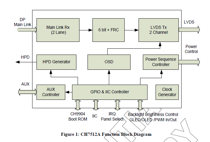
PCB Layout and Design Guide for CH7512A-H, AN-B060 rev0.5
Jun 2026
Chrontel Launches new series of ...
SanJose,CA(June18,2026)—Chrontel(www.chrontel.com), a lead...
Dec 2025
Chrontel Continue upgrading the ...
SanJose,CA(December12,2025)—Chrontel(www.chrontel.com),a leadin...
Copyright © 1998-2017 Chrontel, Inc. All Rights Reserved. Privacy protection Legal statement
